
Edge inference often lives at the intersection of tight power budgets, high video resolutions, and fast iteration cycles. Axelera AI approaches this cross-section with a hardware–software pairing that moves computation closer to memory, keeps model conversion comparatively painless, and treats the entire data path as a single optimisation target. This blog post walks through the architectural choices behind Metis, the design philosophy of the Voyager SDK, and the long-term direction signalled by the Titania chiplet programme.
Digital In-Memory Computing inside Metis
At the level of silicon, Metis replaces the traditional compute-then-fetch cycle with Digital In-Memory Computing (D-IMC). Each 8-bit multiply–accumulate happens inside the same SRAM rows that store the weights, so the energy otherwise spent shuttling data across buses all but disappears. Local RISC-V controllers coordinate the workflow, issuing vector instructions and orchestrating sparsity handling without dragging software developers into micro-architecture details.
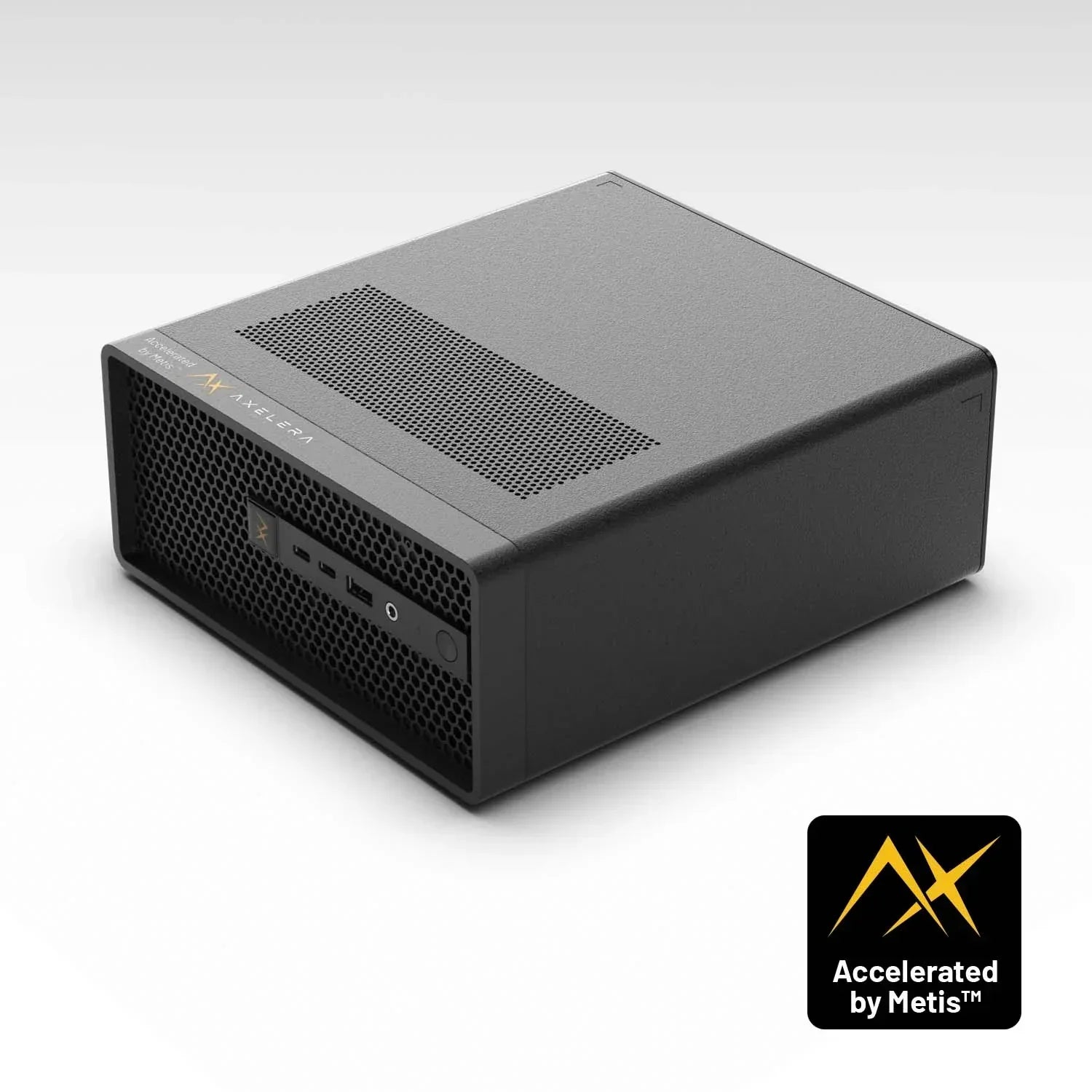
The immediate consequences are easy to measure: a single Metis AIPU sustains north of 200 TOPS while pulling less than ten watts, and the accelerators slot into familiar form factors—M.2 for embedded builds, PCIe for server-class systems.
- Compute where the data is. SRAM rows double as arithmetic units.
- Mixed-precision support. INT8 for bulk layers, INT16 when extra headroom is needed.
- Vector-enabled RISC-V cores. Control flow without proprietary ISA lock-in.
Post-Training Quantisation that Preserves Accuracy
A productive platform must leave room for rapid prototyping, so Axelera leans on post-training quantisation (PTQ) rather than retraining in low precision. Provide roughly a hundred calibration images, let the compiler analyse statistics, and receive an INT8 model whose accuracy typically trails the FP32 baseline by less than a percent. Those calibration passes also guide the compiler’s choice of layer precision: convolutions with narrow dynamic range remain in INT8; numerically sensitive ops stay in INT16. No user intervention required.
| Network | Accuracy loss after PTQ |
|---|---|
| ResNet-50 v1.5 | -0.1 % |
| SSD-MobileNet V1 | -0.3 % |
| YOLOv5s-ReLU | -0.9 % |
Voyager SDK: Piecing the Pipeline Together
Even the quickest AIPU falters if pixels are stuck in format conversions or redundant memory copies. Voyager addresses that by letting developers describe an entire pipeline in one YAML file—H.265 decoding, colour conversion, tiling, inference, post-processing— and compiling it into a zero-copy graph that spans every available device.
Beneath the declarative layer sit two programmable interfaces. AxRuntime exposes buffer allocation and device queues, while AxInferenceNet offers direct model execution. Users who need handcrafted kernels or Vulkan shaders can drop to these layers without leaving the SDK ecosystem.
- YAML pipelines. One file, from camera input to metadata output.
- Zero-copy by default. The builder fuses stages and passes pointers, not images.
- Open lower layers. Extend with CUDA, Vulkan, or custom DSP kernels as needed.
# excerpt: 8 K YOLOv8 pipeline
input:  { source: rtsp://cam, decode: h265 }
tile:   { size: 1280x1280, overlap: 0.15 }
model:  { file: yolov8l_int8.axmodel, device: metis }
output: { overlay: true, stream: ws://localhost:9000 }
A practical demonstration of the approach came at the ISC West security show. An 8 K bullet camera watched the exhibition floor from four metres up, its feed broken into 85 overlapping tiles and processed on two Metis PCIe cards. The system maintained 23 frames per second—about 300 tiles every second—while staying under a 35-watt accelerator budget. Swapping in a lighter YOLO variant brings the workload down to a single card, and an upcoming four-AIPU board will lift the performance ceiling even higher. Impressed? Chech out this accelerator by Axelera.
Titania Chiplets — Scaling without Reinventing the Toolchain
The engineering themes that shape Metis—compute-in-memory, open ISA, mixed precision—carry forward into Titania, a chiplet architecture funded in part by the EuroHPC DARE initiative. Instead of monolithic dies, Titania will assemble many smaller D-IMC tiles behind a standard fabric, delivering edge-to-cloud scalability while letting the existing Voyager toolchain handle placement and scheduling. First boards are expected around 2027; early software compatibility is already baked into the current SDK.
Key Takeaways
- Digital In-Memory Computing removes the bandwidth bottleneck and keeps power low.
- Post-training quantisation converts models in minutes with negligible accuracy cost.
- Voyager pipelines capture every stage from sensor to insight in a single artefact.
- Real-world demos show 8 K detection at practical frame rates and power envelopes.
- The same development flow will carry forward to Titania’s multi-chiplet designs.
Need Guidance on Your Own Build?
Whether you’re evaluating M.2 accelerators for an industrial PC, planning a high-density video analytics rack, or simply exploring quantisation workflows, we can help - and even offer a tailored evaluation setup. Don't hesitate to contact us to discuss your requirements and let us guide you toward the optimal edge AI solution. We look forward to hearing what you are building next.